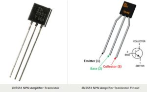
Pin Configuration:
|
Pin Number |
Pin Name |
Description |
|
1 |
Emitter |
Current Drains out through emitter, normally connected to ground |
|
2 |
Base |
Controls the biasing of transistor, Used to turn ON or OFF the transistor |
|
3 |
Collector |
Current flows in through collector, normally connected to load |
Features:
- Amplifier NPN Transistor
- High DC Current Gain (hFE), typically 80 when IC=10mA
- Continuous Collector current (IC) is 600mA
- Collector-Emitter voltage (VCE) is 160 V
- Collector-Base voltage (VCB) is 180V
- Emitter Base Voltage (VBE) is 6V
- Transition Frequency is 100MHz
- Available in To-92 Package
Note: Complete Technical Details can be found at the 2N5551 datasheet given at the end of this page.
Alternative NPN Transistors:
BC549, BC636, BC639, BC547, 2N2369, 2N3055, 2N3904, 2N3906, 2SC5200
2N5551 Equivalent Transistors:
NTE194, 2N5833, 2N5088, 2N3055, 2N5401 (PNP)
Same Family Transistors:
2N5550
Where to use 2N5551:
The 2N5551 is an NPN amplifier Transistor with an amplification factor (hfe) of 80 when the collector current is 10mA. It also has decent switching characteristics (Transition frequency is 100MHz) hence can amplify low-level signals.
Due to this feature, the transistor is commonly used for amplification of audio or other low power signals. So if you are looking for an NPN transistor for you amplifier circuit then this transistor might be the right choice.
How to use 2N5551:
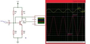
As told earlier the 2N5551 NPN transistor is widely used for amplification. A very simple bare minimum circuit for a transistor to work as an amplifier is shown below. The simulation graph that shows the amplified output sine wave can also be found.

Here the input sine wave of magnitude 8mV (yellow colour) is amplified to 50mV (Pink colour) as shown in the graph. In the above circuit the resistors R3 and R4 form a potential divider which decides the Emitter -Base voltage (VBE). The Resistor R1 is the load resistor and the resistor R2 is the emitter resistor. Changing the value of RL will affect the amplification of the output wave.
A transistor is normally a current amplifier, meaning the current flowing though the base will be amplified in the current flowing through the collector. This amplification depends on the amplification factor (hfe) which is 80 for 2N5551. This means that the collector current will be amplified by 80 times than that of the base current.
Ic = βIb
Another current that we have bring into consideration is the emitter current (IE), but due to transistor action we assume that Emitter current is almost equal to the value of Collector current, however the difference between the both can be found with the value of α. Normally the value of collector current will e given by
IE = IC + IB
The output is obtained across the collector which is the Collector-Emitter voltage (VCE). This output voltage depends on the Input voltage (Vcc, here 12V) without the voltage drop across the loads resistor (R1). Therefore the output voltage Vout can be given as
Vout = VCE = (Vcc – IcRc)
Applications:
- Low power amplifiers
- Current amplifiers
- Small signal boosters
- Audio or other signal amplifiers
- Darlington pair
2D model of the component:
If you are designing a PCD or Perf board with this component then the following picture from the 2N5551 Datasheet will be useful to know its package type and dimensions.
