The most popular and commonly used power electronic switch devices are the Bipolar Junction Transistor BJT and the MOSFET. We have already discussed in detail about the working of BJT and the working of MOSFET and how they are used in circuits. But, both these components had some limitations to be used in very high current applications. So, we moved another popular power electronic switching device called the IGBT. You can think of IGBT as a fusion between BJT and MOSFET, these components have the input characteristics of a BJT and output characteristics of a MOSFET. In this article, we get familiar with the basics of IGBT, how they work, and how to use them in your circuit designs.
What is an IGBT?
IGBT is the short form of Insulated Gate Bipolar Transistor. It is a three-terminal semiconductor switching device that can be used for fast switching with high efficiency in many types of electronic devices. These devices are mostly used in amplifiers for switching/processing complex wave patters with pulse width modulation (PWM). The typical symbol of IGBT along with its image is shown below.
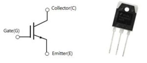
As mentioned earlier an IGBT is a fusion between a BJT and MOSFET. The symbol of the IGBT also represents the same, as you can see the input side represents a MOSFET with a Gate terminal and the output side represents a BJT with Collector and Emitter. The Collector and the Emitter are the conduction terminals and the gate is the control terminal with which the switching operation is controlled.
Internal Structure of IGBT
IGBT can be constructed with the equivalent circuit that consists of two transistors and MOSFET, as the IGBT posses the output of the below combination of the PNP transistor, NPN transistor, and MOSFET. IGBT combines the low saturation voltage of a transistor with the high input impedance and switching speed of a MOSFET. The outcome obtained from this combination delivers the output switching and conduction characteristics of a bipolar transistor, but the voltage is controlled like a MOSFET.
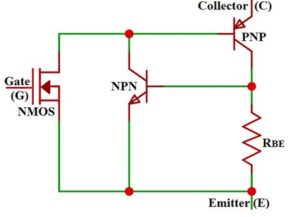
Since IGBT is the combination of MOSFET and BJT they are also called by different names. The different names of IGBT are Insulated Gate Transistor( IGT), Metal Oxide Insulated Gate Transistor (MOSIGT), Gain Modulated Field Effect Transistor (GEMFET), Conductively Modulated Field Effect Transistor (COMFET).
Working of IGBT
IGBT has three terminals attached to three different metal layers, the metal layer of the gate terminal is insulated from the semiconductors by a layer of silicon dioxide (SIO2). IGBT is constructed with 4 layers of semiconductor sandwiched together. The layer closer to the collector is the p+ substrate layer above that is the n- layer, another p layer is kept closer to the emitter and inside the p layer, we have the n+ layers. The junction between the p+ layer and n- layer is called the junction J2 and the junction between the n- layer and the p layer is called the junction J1. The structure of IGBT is shown in the figure below.
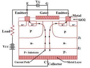
To understand the working of the IGBT, consider a voltage source VG connected positively to the Gate terminal with respect to the Emitter. Consider other voltage source VCC connected across The Emitter and the Collector, where Collector is kept positive with respect to the Emitter. Due to the voltage source VCC the junction J1 will be forward-biased whereas the junction J2 will be reverse biased. Since J2 is in reverse bias there will not be any current flow inside the IGBT(from collector to emitter).
Initially, consider that there is no voltage applied to the Gate terminal, at this stage the IGBT will be in a non-conductive state. Now if we increase the applied gate voltage, due to the capacitance effect on the SiO2 layer the negative ions will get accumulated on the upper side of the layer and the positive ions will get accumulated on the lower side of the SiO2 layer. This will cause the insertion of negative charge carriers in the p region, higher the applied voltage VG greater the insertion of negatively charged carriers. This will lead to a formation of the channel between the J2 junction which allows the flow of current from collector to emitter. The flow of current is represented as the current path in the picture, when the applied Gate voltage VG increases the amount of current flow from the collector to the emitter also increases.
Packages of IGBT
GBTs are available in different kinds of packages with different names from different companies. For example, Infineon Technologies offer Thru-Hole type and Surface mount packages.
- The Thru-hole type package includes TO-262, TO-251, TO-273, TO-274, TO-220, TO-220-3 FP, TO-247, TO-247AD. The surface-mount package includes TO-263, TO-252.
Types of IGBT
The IGBT is classified as two types based on the n+ buffer layer, the IGBTs that are having the n+ buffer layer is called the Punch through IGBT (PT-IGBT), the IGBTs that does not have an n+ buffer layer are called the Non-Punch Through- IGBT (NPT- IGBT).
Based on their characteristics the NPT- IGBT, and PT-IGBT are named as symmetrical and nonsymmetrical IGBTs. The symmetrical IGBTs are the ones that have equal forward and reverse breakdown voltage. The asymmetric IGBTs are the ones that have a reverse breakdown voltage less than the forward breakdown voltage. The symmetrical IGBTs are mostly used in AC circuits, whereas the asymmetrical IGBTs are mostly used in DC circuits because they don’t need to support voltage in the reverse direction.
Difference between Punch through IGBT (PT-IGBT) and Non-Punch Through- IGBT (NPT- IGBT)
|
Punch through IGBT (PT-IGBT) |
Non-Punch Through- IGBT (NPT- IGBT) |
|
These are less rugged in short-circuit failure mode and has less thermal stability
|
These are more rugged in short circuit failure mode and has more thermal stability.
|
|
The collector is a heavily doped P+layer
|
The collector is a lightly doped P-layer.
|
|
It has a small positive temperature coefficient of ON- State voltage, hence parallel operation requires great care and attention.
|
The temperature coefficient of ON-state voltage is strongly positive, hence the parallel operation is easy.
|
|
The turn off loss is more temperature-sensitive, hence it increases significantly at a higher temperature.
|
The turn off a loss is less temperature-sensitive, so, it will remain unchanged with temperature.
|
Operation of IGBT as a Circuit
Since IGBT is a combination of BJT and MOSFET lets look into their operations as a circuit diagram here. The below diagram shows the internal circuit of IGBT which includes two BJT and one MOSFET and a JFET. The Gate, Collector, and Emitter pins of the IGBT are marked below.
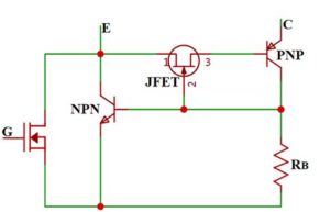
The collector of the PNP transistor is connected to the NPN transistor through a JFET, the JFET connects the collector of the PNP transistor and the base of the PNP transistor. These transistors are arranged in a way to form a parasitic thyristor set up to create a negative feedback loop. The Resistor RB is placed to short the base and emitter terminals of the NPN transistor to ensure that the thyristor doesn’t latch-up which leads to the latch-up of the IGBT. The JFET used here will signify the structure of current between any two IGBT cells and allows the MOSFET and supports most of the voltage.
Switching Characteristics of IGBT
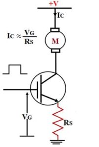
The IGBT is a Voltage controlled device, hence it only requires a small voltage to the gate to stay in the conduction state. And since these are unidirectional devices, they can only switch current in the forward direction which is from collector to emitter. A typical switching circuit of IGBT is shown below, the gate volt VG is applied to the gate pin to switch a motor (M) from a supply voltage V+. The resistor Rs is roughly used to limit the current through the motor.
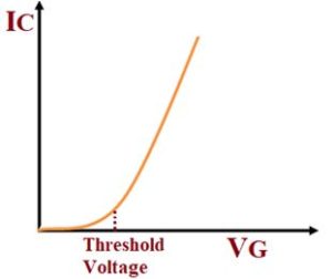
The input characterictcs of IGBT can be understood from the graph below. Initially, when no voltage is applied to the gate pin the IGBT is in turn off condition and no current flows through the collector pin. When the voltage applied to the gate pin exceeds the threshold voltage, the IGBT starts conducting and the collector current IG starts to flow between the collector and emitter terminals. The collector current increases with respect to the gate voltage as shown in the graph below.
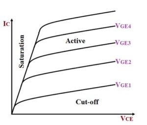
The output characteristics of IGBT have three stages, initially, when the Gate Voltage VGE is zero the device is in the off state, this is called the cutoff region. When VGE is increased and if it is less than the threshold voltage then there will be a small leakage current flowing through the device, but the device will still be in the cutoff region. When the VGE is increased beyond the threshold voltage the device goes into the active region and the current starts flowing through the device. The flow of current will increases with an increase in the voltage VGE as shown in the graph above.
Applications of IGBT
IGBTs are used in various applications such as AC and DC motor drives,
- Unregulated Power Supply (UPS),
- Switch Mode Power Supplies (SMPS),
- traction motor control and induction heating,
- inverters, used to combine an isolated-gate FET for the control input and a bipolar power transistor as a switch in a single device, etc.