It is a Full wave rectifier converts both halves of each waveform cycle into pulsating DC signal using four rectification diodes.
Power Diodes can be connected together to form a full wave rectifier that convert AC voltage into pulsating DC voltage for use in power supplies In the previous Power Diodes tutorial we discussed ways of reducing the ripple or voltage variations on a direct DC voltage by connecting smoothing capacitors across the load resistance.
While this method may be suitable for low power applications it is unsuitable to applications which need a “steady and smooth” DC supply voltage. One method to improve on this is to use every half-cycle of the input voltage instead of every other half-cycle.
Full Wave Rectifier Circuit Diagram
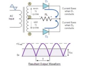
The full wave rectifier circuit consists of two power diodes connected to a single load resistance (RL) with each diode taking it in turn to supply current to the load. When point A of the transformer is positive with respect to point C, diode D1 conducts in the forward direction as indicated by the arrows.
When point B is positive (in the negative half of the cycle) with respect to point C, diode D2 conducts in the forward direction and the current flowing through resistor R is in the same direction for both half-cycles. As the output voltage across the resistor R is the phasor sum of the two waveforms combined, this type of full wave rectifier circuit is also known as a “bi-phase” circuit.
We can see this affect quite clearly if we run the circuit in the Partsim Simulator Circuit with the smoothing capacitor removed.
Simulation Waveform

As the spaces between each half-wave developed by each diode is now being filled in by the other diode the average DC output voltage across the load resistor is now double that of the single half-wave rectifier circuit and is about 0.637Vmax of the peak voltage, assuming no losses.

Where: VMAX is the maximum peak value in one half of the secondary winding and VRMS is the rms value.
The peak voltage of the output waveform is the same as before for the half-wave rectifier provided each half of the transformer windings have the same rms voltage value. To obtain a different DC voltage output different transformer ratios can be used.
The main disadvantage of this type of full wave rectifier circuit is that a larger transformer for a given power output is required with two separate but identical secondary windings making this type of full wave rectifying circuit costly compared to the “Full Wave Bridge Rectifier” circuit equivalent.
The Full Wave Bridge Rectifier
Another type of circuit that produces the same output waveform as the full wave rectifier circuit above, is that of the Full Wave Bridge Rectifier. This type of single phase rectifier uses four individual rectifying diodes connected in a closed loop “bridge” configuration to produce the desired output.
The main advantage of this bridge circuit is that it does not require a special centre tapped transformer, thereby reducing its size and cost. The single secondary winding is connected to one side of the diode bridge network and the load to the other side as shown below.
Merits of Full Wave Rectifier
- The rectification efficiency of full wave rectifiers is double that of half wave rectifiers. The efficiency of half wave rectifiers is 40.6% while the rectification efficiency of full wave rectifiers is 81.2%.
- The ripple factor in full wave rectifiers is low hence a simple filter is required. The value of ripple factor in full wave rectifier is 0.482 while in half wave rectifier it is about 1.21.
- The output voltage and the output power obtained in full wave rectifiers are higher than that obtained using half wave rectifiers.
Diode Bridge Rectifier Circuit Diagram
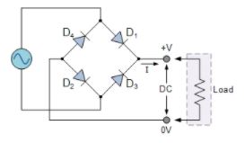
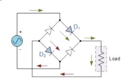
The four diodes labelled D1 to D4 are arranged in “series pairs” with only two diodes conducting current during each half cycle. During the positive half cycle of the supply, diodes D1 and D2 conduct in series while diodes D3 and D4 are reverse biased and the current flows through the load as shown below.
The Positive Half-cycle
During the negative half cycle of the supply, diodes D3 and D4 conduct in series, but diodes D1 and D2 switch “OFF” as they are now reverse biased. The current flowing through the load is the same direction as before.
The Negative Half-cycle
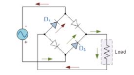
As the current flowing through the load is unidirectional, so the voltage developed across the load is also unidirectional the same as for the previous two diode full-wave rectifier, therefore the average DC voltage across the load is 0.637Vmax.
However in reality, during each half cycle the current flows through two diodes instead of just one so the amplitude of the output voltage is two voltage drops ( 2*0.7 = 1.4V ) less than the input VMAX amplitude. The ripple frequency is now twice the supply frequency (e.g. 100Hz for a 50Hz supply or 120Hz for a 60Hz supply.)
Although we can use four individual power diodes to make a full wave bridge rectifier, pre-made bridge rectifier components are available “off-the-shelf” in a range of different voltage and current sizes that can be soldered directly into a PCB circuit board or be connected by spade connectors.
The image to the right shows a typical single phase bridge rectifier with one corner cut off. This cut-off corner indicates that the terminal nearest to the corner is the positive or +ve output terminal or lead with the opposite (diagonal) lead being the negative or -ve output lead. The other two connecting leads are for the input alternating voltage from a transformer secondary winding.
The Smoothing Capacitor
We saw in the previous section that the single phase half-wave rectifier produces an output wave every half cycle and that it was not practical to use this type of circuit to produce a steady DC supply. The full-wave bridge rectifier however, gives us a greater mean DC value (0.637 Vmax) with less superimposed ripple while the output waveform is twice that of the frequency of the input supply frequency.
We can improve the average DC output of the rectifier while at the same time reducing the AC variation of the rectified output by using smoothing capacitors to filter the output waveform. Smoothing or reservoir capacitors connected in parallel with the load across the output of the full wave bridge rectifier circuit increases the average DC output level even higher as the capacitor acts like a storage device as shown below.
Full-wave Rectifier with Smoothing Capacitor
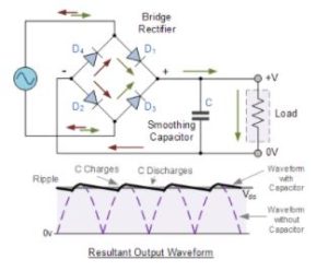
The smoothing capacitor converts the full-wave rippled output of the rectifier into a more smooth DC output voltage. If we now run the Partsim Simulator Circuit with different values of smoothing capacitor installed, we can see the effect it has on the rectified output waveform as shown.
5uF Smoothing Capacitor
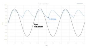
The blue plot on the waveform shows the result of using a 5.0uF smoothing capacitor across the rectifiers output. Previously the load voltage followed the rectified output waveform down to zero volts. Here the 5uF capacitor is charged to the peak voltage of the output DC pulse, but when it drops from its peak voltage back down to zero volts, the capacitor can not discharge as quickly due to the RC time constant of the circuit.
This results in the capacitor discharging down to about 3.6 volts, in this example, maintaining the voltage across the load resistor until the capacitor re-charges once again on the next positive slope of the DC pulse. In other words, the capacitor only has time to discharge briefly before the next DC pulse recharges it back up to the peak value. Thus, the DC voltage applied to the load resistor drops only by a small amount. But we can improve this still by increasing the value of the smoothing capacitor as shown.
50uF Smoothing Capacitor
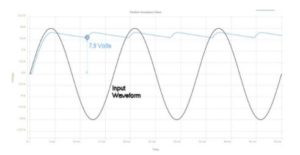
Here we have increased the value of the smoothing capacitor ten-fold from 5uF to 50uF which has reduced the ripple increasing the minimum discharge voltage from the previous 3.6 volts to 7.9 volts. However, using the Partsim Simulator Circuit we have chosen a load of 1kΩ to obtain these values, but as the load impedance decreases the load current increases causing the capacitor to discharge more rapidly between charging pulses.
The effect of a supplying a heavy load with a single smoothing or reservoir capacitor can be reduced by the use of a larger capacitor which stores more energy and discharges less between charging pulses. Generally for DC power supply circuits the smoothing capacitor is an Aluminium Electrolytic type that has a capacitance value of 100uF or more with repeated DC voltage pulses from the rectifier charging up the capacitor to peak voltage.
Bridge Rectifier Ripple Voltage

Where: I is the DC load current in amps, ƒ is the frequency of the ripple or twice the input frequency in Hertz, and C is the capacitance in Farads.
The main advantages of a full-wave bridge rectifier is that it has a smaller AC ripple value for a given load and a smaller reservoir or smoothing capacitor than an equivalent half-wave rectifier. Therefore, the fundamental frequency of the ripple voltage is twice that of the AC supply frequency (100Hz) where for the half-wave rectifier it is exactly equal to the supply frequency (50Hz).
The amount of ripple voltage that is superimposed on top of the DC supply voltage by the diodes can be virtually eliminated by adding a much improved π-filter (pi-filter) to the output terminals of the bridge rectifier. This type of low-pass filter consists of two smoothing capacitors, usually of the same value and a choke or inductance across them to introduce a high impedance path to the alternating ripple component.