A MOSFETs exhibit three regions of operation viz., Cut-off, Linear or Ohmic and Saturation. Among these, when MOSFETs are to be used as amplifiers, they are required to be operated in their ohmic region wherein the current through the device increases with an increase in the applied voltage. On the other hand, when the MOSFETs are required to function as switches, they should be biased in such a way that they alter between cut-off and saturation states. This is because, in cut-off region, there is no current flow through the device while in saturation region there will be a constant amount of current flowing through the device, just mimicking the behaviour of an open and closed switch, respectively. This functionality of MOSFETs is exploited in many electronic circuits as they offer higher switching rates when compared to BJTs (bipolar junction transistors).
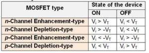
Figure 1 shows a simple circuit which uses an n-channel enhancement MOSFET as a switch. Here the drain terminal (D) of the MOSFET is connected to the supply voltage VS via the drain resistor RD while its source terminal (S) is grounded. Further, it has an input voltage Vi applied at its gate terminal (G) while the output Vo is drawn from its drain.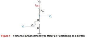
Now consider the case where Vi applied is 0V, which means the gate terminal of the MOSFETis left unbiased. As a result, the MOSFET will be OFF and operates in its cutoff region wherein it offers a high impedance path to the flow of current which makes the IDS almost equivalent to zero. As a result, even the voltage drop across RD will become zero due to which the output voltage Vo will become almost equal to VS.
Next, consider the case where the input voltage Vi applied is greater than the threshold voltage VT of the device. Under this condition, the MOSFET will start to conduct and if the VS provided is greater than the pinch-off voltage VP of the device (usually it will be so), then the MOSFET starts to operate in its saturation region. This further means that the device will offer low resistance path for the flow of constant IDS, almost acting like a short circuit. As a result, the output voltage will be pulled towards low voltage level, which will be ideally zero.
From the discussion presented, it is evident that the output voltage alters between VS and zero depending on whether the input provided is less than or greater than VT, respectively. Thus, it can be concluded that MOSFETs can be made to function as electronic switches when made to operate between cut-off and saturation operating regions.
Similar to the case of n-channel enhancement type MOSFET, even n-channel depletion type MOSFETs can be used to perform switching action as shown by Figure 2. The behaviour of such a circuit is seen to be almost identical to that explained above except the fact that for cut-off, the gate voltage VG needs to be made negative and should be lesser than -VT.
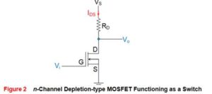
Next, Figure 3 shows the case wherein the p-channel enhancement MOSFET is used as a switch. Here it is seen that the supply voltage VS is applied at its source terminal (S) and the gate terminal is provided with the input voltage Vi while the drain terminal is grounded via the resistor RD. Further the output of the circuit Vo is obtained across RD, from the drain terminal of the MOSFET.
In the case of p-type devices the conduction current will be due to holes and will thus flow from source to drain ISD, and not from drain to source (IDS) as in the case of n-type devices. Now, let us assume that the input voltage which is nothing but the gate voltage VG of the MOSFET goes low. This causes the MOSFET to switch ON and to offer a low (almost negligible) resistance path to the current flow. As a result heavy current flows through the device which results in a large voltage drop across the resistor RD. This inturn results in the output which is almost equal to the supply voltage VS.
Next, consider the case where Vi goes high i.e. when Vi will be greater than the threshold voltage of the device (VT will be negative for these devices). Under this condition, the MOSFET will be OFF and offers a high impedance path for the current flow. This results in almost zero current leading to almost zero voltage at the output terminal.
Similar to this, even p-channel depletion-type MOSFETs can be used to perform switching action as shown by Figure 4. The working of this circuit is almost similar to the one explained above except for the fact that here the cut-off region is experienced only if Vi = VG is made positive such that it exceeds the threshold voltage of the device.
The table presented below summarizes the discussion presented above.