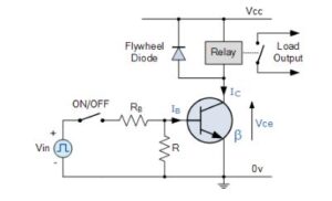
We are transistor as a switch can be extensively used for switching operations, either for opening or closing a circuit. On the other hand, the basic concept behind the operation of a transistor as a switch relies on its mode of operation. Generally, the low-voltage DC is turned on or off by transistors in this mode.
Both PNP and NPN transistors can be Utilised as switches. A basic terminal transistor can be handled differently from a signal amplifier by biasing both NPN and PNP bipolar transistors with an “ON / OFF” static switch. One of the main uses of the transistor to transform a DC signal “ON” or “OFF” is solid-state switches.
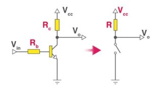
Basic of NPN Transistor Switching Circuit diagram
The circuit resembles that of the Common Emitter circuit we looked at in the previous tutorials. The difference this time is that to operate the transistor as a switch the transistor needs to be turned either fully “OFF” (cut-off) or fully “ON” (saturated).
An ideal transistor switch would have infinite circuit resistance between the Collector and Emitter when turned “fully-OFF” resulting in zero current flowing through it and zero resistance between the Collector and Emitter when turned “fully-ON”, resulting in maximum current flow.
when the transistor is turned “OFF”, small leakage currents flow through the transistor and when fully “ON” the device has a low resistance value causing a small saturation voltage ( VCE ) across it. Even though the transistor is not a perfect switch, in both the cut-off and saturation regions the power dissipated by the transistor is at its minimum.
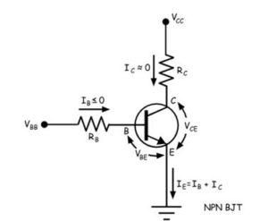
In order for the Base current to flow, the Base input terminal must be made more positive than the Emitter by increasing it above the 0.7 volts needed for a silicon device. By varying this Base-Emitter voltage VBE, the Base current is also altered and which in turn controls the amount of Collector current flowing through the transistor as previously discussed.
When maximum Collector current flows the transistor is said to be Saturated. The value of the Base resistor determines how much input voltage is required and corresponding Base current to switch the transistor fully “ON”.
In a transistor Switch Working characteristic,
there are three Types of regions,
- Active Region
- Saturation Region
- Cutoff Region

In the active region, for wide range of collector-emitter voltage (VCE) collector current (IC) remains constant. As the voltage has a wide range and collector current is almost constant, there will be significant power loss if the transistor is operated in this region. When an ideal switch is OFF, the current is zero hence there is no power loss.
Similarly, when the switch is ON, the voltage across the switch is zero hence, there is no power loss again. When we want a BJT to be operated as a switch, it must be operated in such a way that the power loss during ON and OFF condition should be nearly zero, or very low.
It is only possible when the transistor is only operated in the marginal region of the characteristics. The cutoff region and saturation region are two marginal regions in the transistor characteristics. Note that this applies to both npn transistors and pnp transistors.
In the figure, when base current is zero, the collector current (IC) has very small constant value for a wide range of collector-emitter voltage (VCE). So when the transistor is operated with base current ≤ 0, the collector current (IC ≈ 0) is very tiny, hence the transistor is said to be in OFF condition but at the same time, power loss across the transistor switch i.e. IC × VCE is negligible because of very tiny IC.
2.Saturation Region
The transistor is connected in series with an output resistance RC. Hence, current through the output resistance is

If the transistor is operated with a base current IB3 for which collector current is IC1. IC is less than IC1, then the transistor is operated in the saturation region. Here, for any collector current less than IC1, there will be very tiny collector-emitter voltage (VCE < VCE1). Hence in this situation, the current through the transistor is as high as load current, but the voltage across the transistor (VCE < VCE1) quite low, hence power loss in the transistor is negligible.

The transistor behaves as an ON switch. So for using the transistor as a switch we should make sure that the applied base current must be sufficiently high to Keep the transistor in the saturation region, for a collector current
3.Cut-off Region

So, from the above explanation, we can conclude that bipolar junction transistor behaves as a switch only when it is operated in the cutoff and saturation region of its characteristic. In switching application, the active region or active region of characteristics is avoided. As we already told, the power loss in transistor switch is very low but not zero. So, it is not an ideal switch but accepted as a switch for specific applications.
When we choose a transistor as a switch, we have to care about the rating of the transistor. Because during ON condition, the entire load current will flow through the transistor, if this current is more than a safe value of collector-emitter current carrying capacity of the transistor, then the transistor may be permanently destroyed due to overheating. Again at OFF condition, the entire open circuit voltage of the load will appear across the transistor. The transistor must be able to withstand this voltage otherwise collector-emitter junction will break down and transistor becomes ‘ON’ instead of being ‘OFF’. Another thing must be considered during a transistor as a switch. A heat sink of suitable size and design is always required with the transistor. Each transistor takes a finite time to go from OFF to ON condition and vice verse.
Although this finite time is very small, maybe less than few microseconds but still, it is not zero. During switch ON period, the current (IC) will be building up while the collector-emitter voltage VCE will be falling towards zero. As the current increases from zero (ideal) to its maximum value and voltage falls from the maximum value to zero (ideal) there will be an instant where both of them will be maximum. At that point, peak power loss happens. In the same way, maximum power loss happens in a transistor when it comes at OFF state from ON state. Hence maximum power loss happens in a transistor during the transition period of changing state but still, the amount of energy dissipated is quite moderate as the period of transition is quite small. For low-frequency operation, the generated heat may be moderated. But if the frequency of operation is quite high, there will be significant power loss and corresponding generation of heat.
This is to be noted that, heat generation does not occur only during transient condition also during steady ON or OFF condition of the transistor but the amount of heat during steady condition is quite.