A transistor is a type of a semiconductor device that can be used to both conduct and insulate electric current or voltage. A transistor basically acts as a switch and an amplifier. In simple words, we can say that a transistor is a miniature device that is used to control or regulate the flow of electronic signals.
Transistors are one of the key components in most of the electronic devices that are present today. Developed in the year 1947 by three American physicists John Bardeen, Walter Brattain and William Shockley, the transistor is considered as one of the most important inventions in the history of science.
Parts of a Transistor
A typical transistor is composed of three layers of semiconductor materials or more specifically terminals which helps to make a connection to an external circuit and carry the current. A voltage or current that is applied to anyone pair of the terminals of a transistor controls the current through the other pair of terminals. There are three terminals for a transistor. They are;
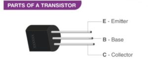
- Base: This is used to activate the transistor.
- Collector: It is the positive lead of the transistor.
- Emitter: It is the negative lead of the transistor.
Well, the very basic working principle of a transistor is based on controlling the flow of current through one channel by varying intensity of a very smaller current that is flowing through a second channel.
Types of Transistors
Based on how they are used in a circuit there are mainly two types of transistors.
- BJT (Bipolar Junction Transistor)
- FET (Field Effect Transistor)
1.Bipolar Junction Transistor (BJT)
The three terminals of BJT are base, emitter and collector. A very small current flowing between base and emitter can control a larger flow of current between the collector and emitter terminal.
Furthermore, there are two types of BJT. These include;
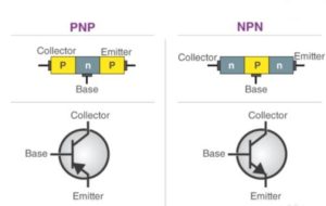
- P-N-P Transistor: It is a type of BJT where one n-type material is introduced or placed between two p-type materials. In such a configuration, the device will control the flow of current. PNP transistor consists of 2 crystal diodes which are connected in series. The right side and left side of the diodes are known as the collector-base diode and emitter-base diode respectively.
- N-P-N Transistor: In this transistor, we will find one p-type material that is present between two n-type materials. N-P-N transistor is basically used to amplify weak signals to strong signals. In NPN transistor, the electrons move from the emitter to collector region resulting in the formation of current in the transistor. This transistor is widely used in the circuit.
There are three types of configuration as a
A. common base (CB),
B. common collector (CC) and
C. common emitter (CE).
In Common Base (CB) configuration the base terminal of the transistor is common between input and output terminals.
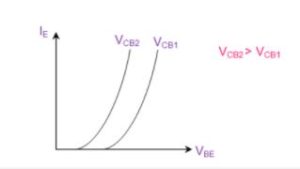
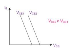
A. Common base (CB) Configuration

Input Characteristics
CB Configuration
This chart will describe the variation of emitter current, IE with base – Emitter voltage, VBE keeping collector voltage constant, VCB.
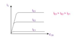
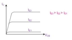
Output Characteristics
CB Configuration
This chart shows the variation of collector current, IC with VCB by keeping emitter current IE constant.
B. Common Collector(CC) Configuration
In Common Collector (CC) configuration the collector terminals are common between the input and output terminals.
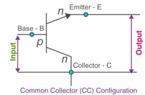
Input Characteristics
It shows the variation in IB in accordance with VCB with collector-emitter voltage VCE keeping constant.
Output Characteristics
This exhibit the variation in IE against the changes in VCE by keeping IB constant.
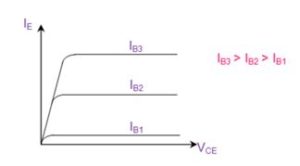
C. In Common Emitter (CE) configuration
In Common Emitter (CE) configuration the emitter terminal is common between the input and the output terminals.
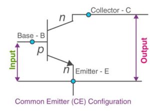
Input Characteristics
Here it shows the variation in IC with the changes in VCE by keeping IB constant.

Output Characteristics
Here it shows the variation in IC with the changes in VCE by keeping IB constant.
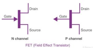
2. Field Effect Transistor (FET)
For FET, the three terminals are Gate, Source and Drain. The voltage at the gate terminal can control a current between source and drain. FET is a unipolar transistor in which N channel FET or P channel FET are used for conduction. The main applications of FETs are in low noise amplifier, buffer amplifier and an analogue switch.
Other Types
Apart from these, there are many other types of transistors which include MOSFET, JFET, insulated-gate bipolar transistor, this film transistor, high electron mobility transistor, inverted-T field-effect transistor (ITFET), fast-reverse epitaxial diode field-effect transistor (FREDFET), Schottky transistor, tunnel field-effect transistor, organic field-effect transistor (OFET), diffusion transistor, etc.
How do Transistors work?
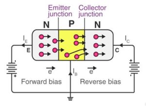
Let us look at the working of transistors. We know that BJT consists of three terminals (Emitter, Base and Collector). It is a current-driven device where two P-N junctions exist within a BJT.
One P-N junction exists between emitter and base region and the second junction exists between the collector and base region. A very small amount of current flow through emitter to the base can control a reasonably large amount of current flow through the device from emitter to collector.
In usual operation of BJT, the base-emitter junction is forward biased and the base-collector junction is reverse biased. When a current flows through the base-emitter junction, a current will flow in the collector circuit.
In order to explain the working of the transistor, let us take an example of an NPN transistor. The same principles are used for PNP transistor except that the current carriers are holes and the voltages are reversed.
Operation of NPN Transistor
The emitter of NPN device is made by n-type material, hence the majority carriers are electrons. When the base-emitter junction is forward biased the electrons will move from the n-type region towards the p-type region and the minority carriers holes moves towards the n-type region.
When they meet each other they will combine enabling a current to flow across the junction. When the junction is reverse biased the holes and electrons move away from the junction, and now the depletion region forms between the two areas and no current will flows through it.
When a current flows between base and emitter the electrons will leave the emitter and flow into the base as shown above. Normally the electrons will combine when they reach the depletion region.
But the doping level in this region is very low and the base is also very thin. Which means that most of the electrons are able to travel across the region without recombining with holes. As a result, the electrons will drift towards the collector.
By this way, they are able to flow across what is effectively reverse-biased junction and the current flows in the collector circuit.
Advantages of Transistor
- Lower cost and smaller in size.
- Smaller mechanical sensitivity.
- Low operating voltage.
- Extremely long life.
- No power consumption.
- Fast switching.
- Better efficiency circuits can be developed.
- Used to develop a single integrated circuit.
Limitations of Transistors
Transistors also have few limitations. They are as follows;
- Transistors lack higher electron mobility.
- Transistors can be easily damaged when electrical and thermal events arise. For example, electrostatic discharge in handling.
- Transistors are affected by cosmic rays and radiation.